Double Side
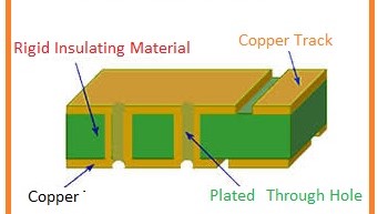
Double Sided PCB, also known as two layer PCB is a type of PCB which has conductive copper layers on both sides of the board i.e. top and bottom It is extremely useful in many electronic applications because circuits on one side of the board can be connected on the other side of the board with the help of holes drilled on the board which needs platting in holes(PTH) Components on these boards can be connected using two different useful technologies i.e. Through Hole Technology and Surface Mount Technology based on the needs and requirements, both technologies come with their own benefits and limitations. There exists a silk screen above solder mask on both side of the board which is mainly used for adding symbols and characters on the board so a common person can understand the board functions.